
At the OPEnS Lab, we’ve found a common requirement amongst our projects: a long, long, long battery life. The OPEnSampler was particularly challenging due to its simultaneous 3.3V, 5V, and 12V power requirements. MOSFET circuits exist that can manipulate power sources and drop their standby currents to near-zero, but designing these in a way that latched their state in both directions, and were powered exclusively from the source battery, was difficult. This short blog post will discuss the features and considerations of Release 1.0.0 of the OPEnS Power Control Board.

The schematic
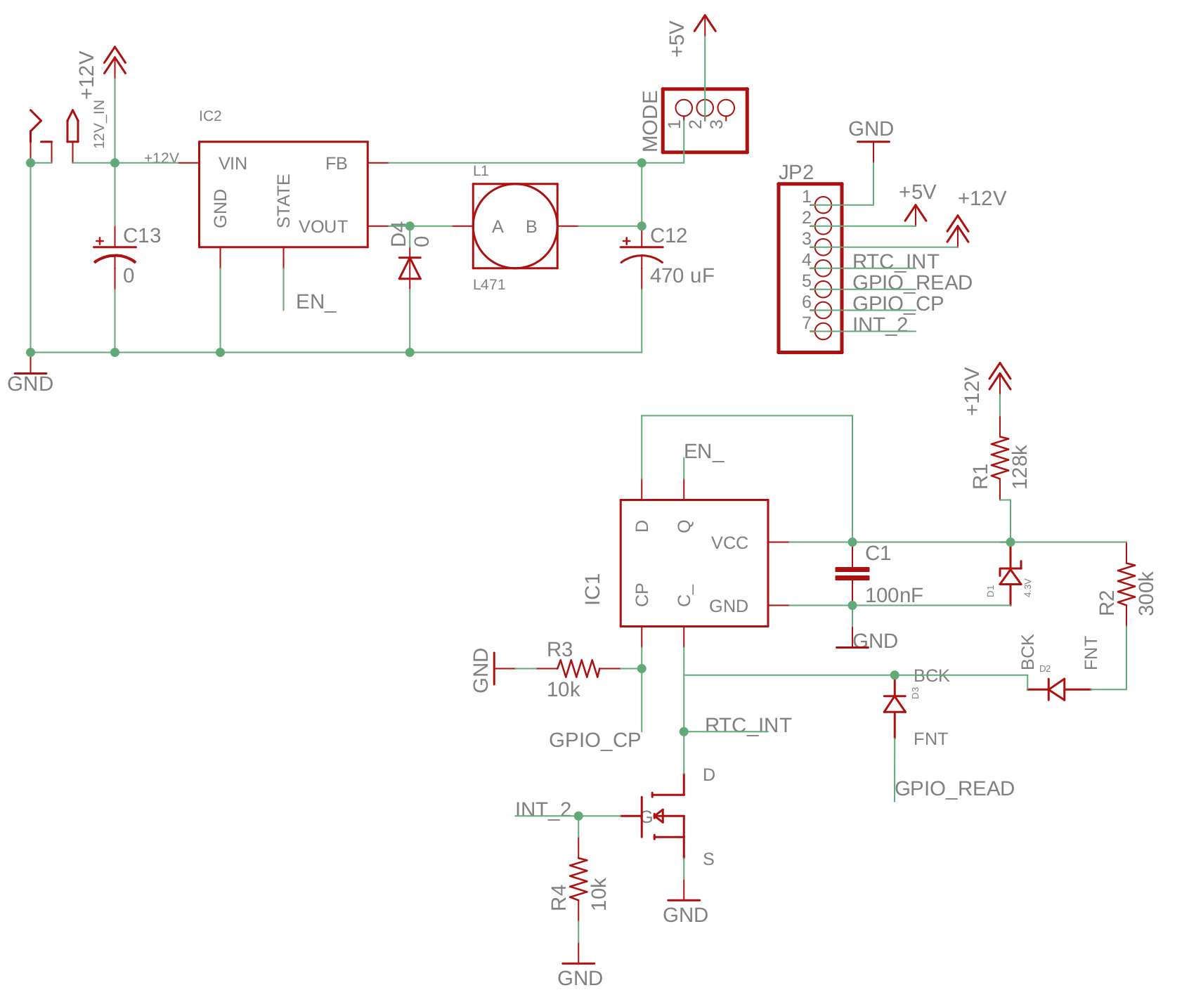
The circuit was designed by Mitch Nelke. There are two core integrated circuits in this board. IC1 represents the flip flop IC and is responsible for latching its EN-bar output HIGH or LOW after a HIGH pulse on its Clock Pulse input or a LOW pulse on its C-bar input, respectively. IC2 represents the 12v-5v switching regulator component that drops the battery’s 12v supply to the 5v used to power the microcontroller and other components.
The Flip Flop
The flip flop circuit power is sourced from the battery’s raw 12v, though it is dropped down to 4.3v by the zener diode D1. R1 was chosen based on a minimum required current of 60uA, derived from the max required input current of the switching regulator’s enable pin and the current required by the flip flop IC plus a bit of extra as a buffer. This 4.3v source is also used to pull the flip flop’s D input HIGH at all times. The Clock Pulse (CP) input is pulled to ground by a 10k resistor. On a rising edge on CP, the flip flop reads the boolean state of D and sets its Q output to match that value. With this setup, a HIGH pulse to CP will always set Q HIGH.
The C-bar input has a weak pullup resistor, R2, to 4.3v. When C-bar is pulled LOW, such as through the RTC_INT input or a HIGH input from INT_2, the flip flop IC ignores any clock pulses and sets its Q output LOW. When C-bar is raised HIGH, Q will stay LOW until the next clock pulse.
GPIO_READ allows a microcontroller input pin to read the state of the real time clock’s (RTC) interrupt alarm while the device is on. RTC_INT should be attached directly to the RTC’s INT/SQW pin, and GPIO_CP should be attached to the microcontroller’s output pin that is responsible for shutting the device off.
The Switching Regulator
The switching regulator efficiently converts the 12v input to a 5v output. This part of the circuit is essentially ripped from the LM2575 datasheet’s recommended circuit. Its EN-bar input acts as a low-true output-enable and is attached directly to the flip flop’s Q output. The 5v output of the regulator is fed through the MODE jumper. The MODE jumper’s first two pins should be connected during regular use, but should be disconnected when a USB is plugged into the microcontroller (to program it, for example) to not have competing 5v supplies.
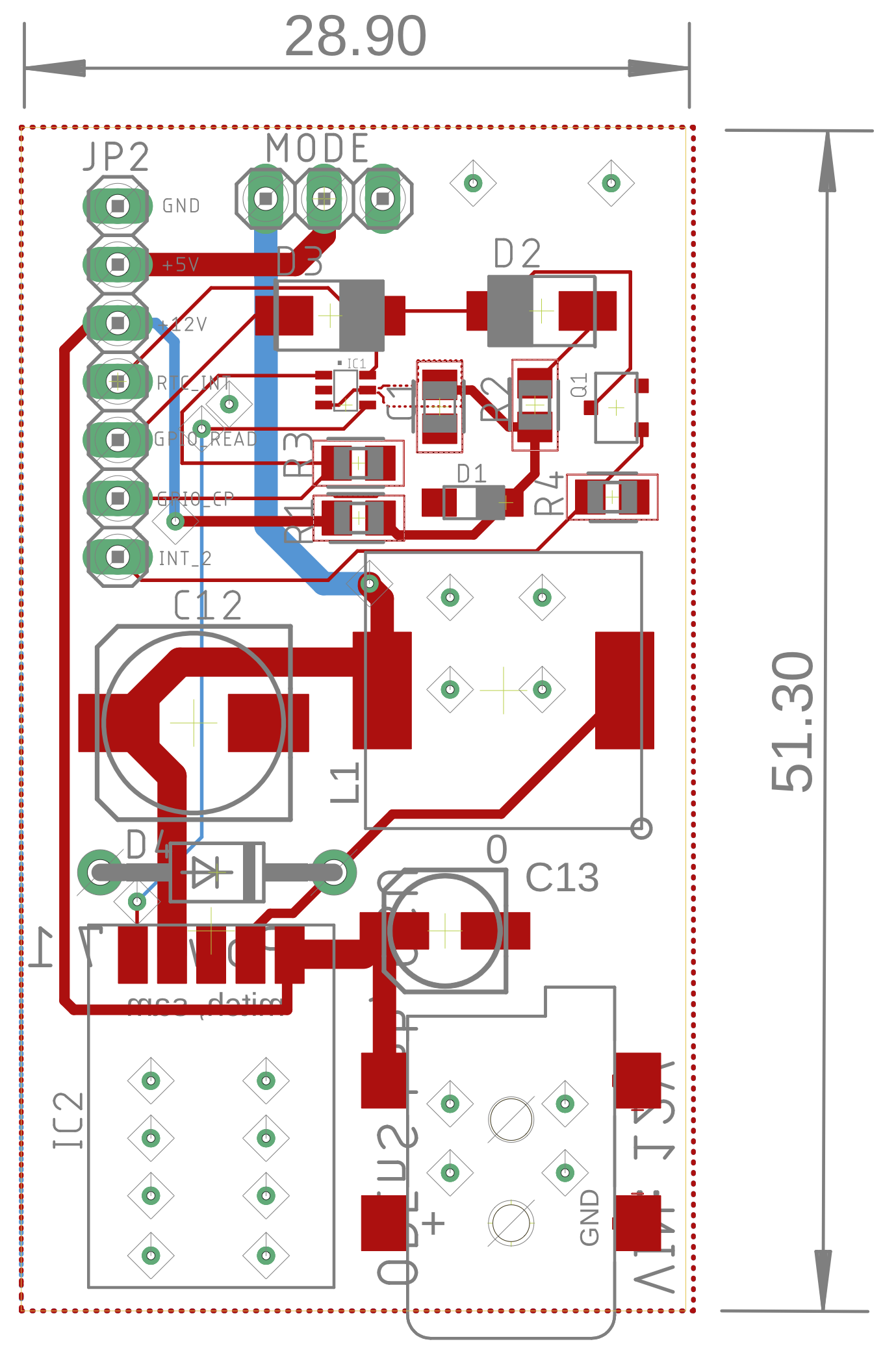
The Board
The board layout was done in EAGLE CAD by Sam Edwards. I’ve added dimensions and turned off tStop and pour planes so it is more clear.
Connections
The board is designed specifically to work with Adafruit’s Feather M0 microcontroller series. It should be powered by a 12v battery plugged into the 2.5×5.5mm barrel jack receptacle.
-
The +5V pin should connect to the M0’s USB power pin or the Arduino Uno’s Vin. MODE should be closed with a jumper to enable the 5v output of the board.
-
The +12V output should be connected to any circuitry that requires 12v.
-
RTC_INT should be connected to the real time clock’s interrupt output, or any other independent circuitry that sends a LOW-TRUE signal to turn the device on.
-
GPIO_READ should be connected to an input pin on the microcontroller if the real time clock’s alarm needs to be read by the microcontroller when power is already enabled.
-
GPIO_CP should be connected to the microcontroller’s digital output that is designated as the shutoff pin.
-
INT2 should be connected to any external circuitry that should power the device on with a HIGH-TRUE signal.
Testing
A current draw test was conducted by measuring the current with a multimeter between the battery’s positive lead and the positive input on the power control board. The power control board was attached to the OPEnSampler’s Microcontroller Breakout Board, upon which Adafruit’s Feather M0 Wifi microcontroller was also attached. The microcontroller was programmed ahead of time to simply power its LED upon powering up. One jumper cable was connected to the real time clock’s 3v3 power pin, supplied by the M0, and was temporarily connected to the power control board’s GPIO_CP pin to turn the device off. Another jumper cable was connected to ground and RTC_INT to turn the device on.
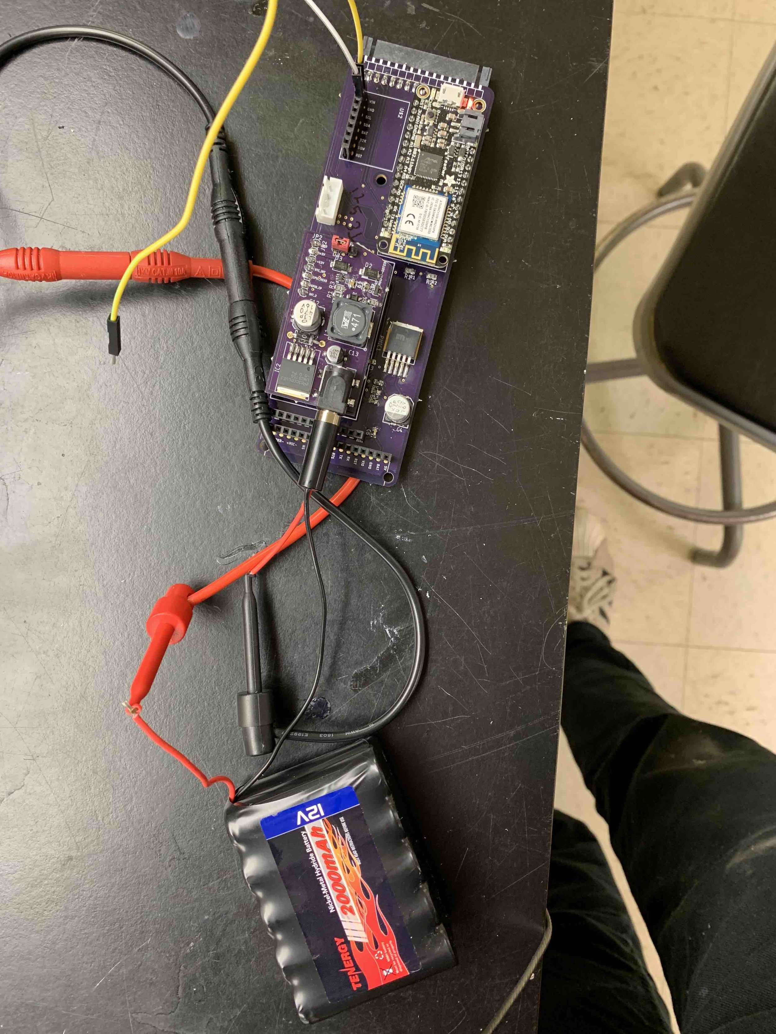
The device had a current draw of 22mA when powered on and only 130uA when powered off. When powered by the small 2000mAH, 12v battery used on the OPEnSampler, the device will have a maximum standby battery life of 641 days (not accounting for the battery’s internal leakage current). If the device had used normal sleep methods that can reduce the consumption down to 1.5mA, the maximum standby life would have only been 55 days. With no standby mode at all, the battery life would have been less than four days.
Considerations
An important consideration is that I am not an electrical engineer, nor am I pursuing a degree in electrical engineering. There is much to be improved on this board, and if you have any ideas, or find a bug in its design, you shouldn’t hesitate to contact the OPEnS Lab or leave a comment on this post! Additionally, this was only tested on Adafruit’s Feather M0 Wifi breakout, so your mileage may vary on other boards (especially ones that are not in the Feather M0 family!).
Finally, when using this board it is important to understand that the microcontroller is completely shut down on “standby” mode. This means that after the real time clock wakes the device up, it will start at the setup routine and any variables stored in flash will be erased. Be sure to use non-volatile storage methods for variables that must be saved between power cycles. The OPEnS Power board, for example, includes a small EEPROM chip. Adafruit’s Feather M0 Express includes extra SPI or QSPI flash memory that isn’t erased between power cycles as well.
Conclusion
The primary application of the OPEnS Power Control Board is to increase the battery life of a sensor suite powered by a 12v, 2000mAH battery. This board is capable of dropping the standby current of microcontroller-based projects down to 130 micro-amps. The minimum standby current that could be achieved previously was about 1.5mA based on Adafruit’s tutorial linked previously. The OPEnS Power Control Board increased the theoretical max standby battery life from 55 days to 641 days. The device fully shuts off on standby and wakes up from pulses to either of its two interrupt vectors, one HIGH-TRUE and one LOW-TRUE.
![]()
Written by Mitch Nelke, OPEnS Lab OSU